


Our experts
Explore our diverse range of expertise.
.jpg)
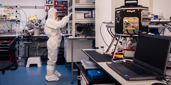
Cutting-edge interdisciplinary research and innovation to deliver real-world impact
The strength and breadth of our fundamental research is reflected in eight core themes that champion originality, rigour, and excellence.
We’re keen to ensure that industries have access to all the school can offer, whether it’s finding the best graduate engineers and physicists, developing a product, using our facilities, or carrying out collaborative research.
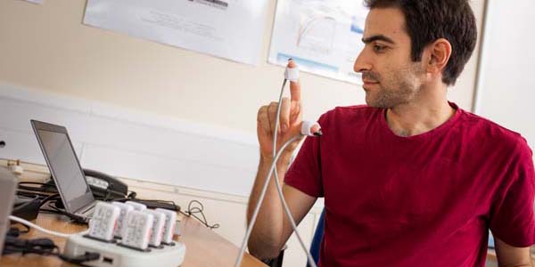
ClearSky Medical Diagnostics specialises in medical devices for the diagnosis and monitoring of Parkinson’s, Alzheimer’s and a range of other neurodegenerative conditions.
Our academics undertake a wide range of commercialisation and consultancy activities, which have led to the following spin-out companies:
From self-playing instruments to policy work for the creative industries, Jay's work bridges the divide between artistic expression and industrial data.
Navigating this unconventional, dual trajectory has required adaptability and resourcefulness, something that Jay has embraced with openness and enthusiasm.