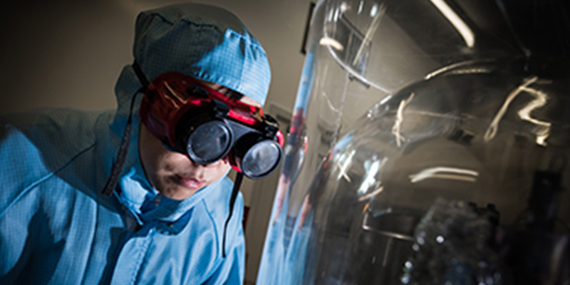
The engineering cleanroom
Our engineering cleanroom is available for use by staff and students in the School and by local business.
Quick facts
- The facility is validated to ISO6 (Class 1,000) in the wafer processing room and ISO5 (class 100) under the laminar flow filter units therein. The larger process lab conforms to ISO7 (class 10,000), while the entry room conforms to ISO8 (class 100,000).
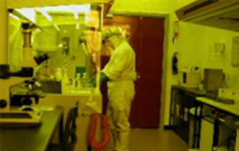
- It was completed in 1989 and refurbished in 2022 to support teaching and research activities. Research areas include the fabrication and characterisation of electronic, bio-electronic, fluidic and micro-mechanical devices.
- Students fabricate their own devices on various substrates during group teaching activities. In addition, the cleanroom and associated facilities my be used by undergraduate and postgraduate students during individual project work.
The cleanroom offers:
- dust-free assembly
- solid-state electronics, micro-mechanical and micro-fluidic fabrication
- nano-fabrication
- analytical instruments for characterising nanoscale devices.
Preparation
- Thermal Oxidation Furnace - a furnace is available for the wet oxidation of silicon wafers up to four inches diameter.
- Evaporator - a variety of metals can be deposited onto a substrate from a molten source in a vacuum. Bell jar diameter = 29cm.
- Plasma reactive ion etcher (RIE) - a plasma reactive ion etcher is used to excite gases in order to etch materials such as silicon, gallium arsenide, aluminium and films of organic materials (in particular, photoresists, used to create nanopatterned materials).
Fabrication
Mask alignment photolithography
- The cleanroom suite has an ultra-clean ISO5 room with low airborne particle concentrations.
- The room is equipped with fume extracted lamina flow benches and filtered amber lighting for photolithography.
- Equipment includes a mask-aligner (up to four inch wafers), a photoresist spinner, UV ozone cleaner, a wet chemical workstation and a high power optical microscope with frame grabber and measurement capabilities.
Other fabrication tools:
- Wire bonder - the wedge bonder will bond gold and aluminium wire for device connection to package pins
- Silicon micro-machining - wet chemical etching, as well as reactive ion etching, can be used to produce small "micro-machined" objects based on silicon single crystal wafers
- Bench space - we can offer bench space for the assembly of components in a clean environment. Area = 1m x 0.6m.
Measurement
Step profiler
This instrument is used to check layer thickness:
- Range = 1000Å - 1000KÅ
- Resolution = 50Å
- Accuracy = 1% of range.
Measurement tools for the characterisation of devices:
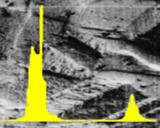
- AFM - an atomic force microscope (AFM) is available. This instrument can measure samples of 1cm2. It can resolve nanoscale features and produce 2D and 3D images.
- Hall effect probe station - his can measure magneto-resistance, sheet-resistance and the Hall effect on various samples. The samples can be cooled with liquid nitrogen to minimise thermal noise during measurement.
- Micro manipulator probe station - fine probe needles are employed to measure resistance, and diode and transistor characteristics in the x – y plane.
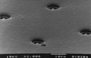
- Scanning electron microscope - an electron microscope is available for the examination of structures. Resolution 3-5 nm. A photo-spectrometer is available to measure the transmission, reflectivity and absorption of thin film devices.