School of Physics, Engineering and Technology
Nanodevices and nanofab: projects
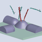
Nanoelectronic Biosensors
Members: S D Johnson
Website: http://www-users.york.ac.uk/~sdj507/BiomolecularElectronics/nanoelectronic_biosensors.html
Funded by: BBRC, HITACHI
Start Date: January 2013
Our understanding of biological science is based predominately on many decades of study on large ensembles of molecules. Bioscience today has become increasingly focused on the properties and function of individual biomolecules. The earliest demonstration of a single molecule experiment emerged from a union of electronics with biology that enabled the conductance of a single transmembrane ion channel to be measured.
We have shown recently that a perturbation of a molecular layer formed on an electrode, for example a change in molecular conformation or the formation of a protein-ligand complex, can be detected electronically through measurements of the electrochemical impedance. However, direct electrochemical impedance measurements are limited in sensitivity and restricted to measurements of the average response of molecular ensembles. In order to interrogate biomolecular function at the single molecule level, it is necessary to adopt alternative electronic technology in which conductance is critically and sensitively dependent on the system impedance.
Single electron transistors (SETs) are reminiscent of field-effect transistors – the basis of all modern electronics – but SET conductivity can be modulated by several orders of magnitude upon the addition of just a single electron. Our commercial partner, Hitachi Cambridge Laboratory Ltd, have pioneered the design and characterisation of SETs that can be fabricated using conventional CMOS compatible processing. Critically, they act as highly sensitive detectors of charge, and accordingly impedance, with sub-single electron charge sensitivity. This extremely high sensitivity to the local environment coupled with comparable size between the SET and many biological macromolecules (SET diameter typically <50 nm compared to around 14 nm for long axis of IgG), opens the possibility of label-free electronic detection at the single molecule level. Furthermore, they can be assembled in high-density arrays and designed to operate on microsecond time enabling multiplexed bioanalysis with high temporal resolution. This highly interdisciplinary programme will investigate approaches for integrating molecular biology with SETs in order to demonstrate in-vitro detection of biochemical activity at the single molecule level.
Artificial Regulation of Biochemical Activity

Members: S D Johnson
Website: http://www-users.york.ac.uk/~sdj507/BiomolecularElectronics/biochemical_regulation.html
Start Date: December 2012
Biomolecules have an impressive range of physical and functional properties, from molecular recognition and mechanical strength, to photosynthesis and force generation. The aim of biomolecular electronics is to create a fusion of biology and electronics that brings these powerful biological attributes to the pervasive, inorganic world of electronics. Existing realisations of this emerging technology are to date essentially ‘static’; biomolecular function is invariable and predetermined according to the specific immobilised biomolecule. In contrast, biological systems have evolved complex regulatory controls that allow the function of molecules to be switched on and off in response to specific stimuli. We are thus investigating dynamic and switchable biomolecular electronic devices that can activate and regulate biomolecular properties in response to local electric fields. This is a highly inter-disciplinary project involving collaboration with chemists and molecular biologists across the University.
Self-assembled Nanosphere Lithography
Members: Dr. Yongbing Xu, Mr. Daxin Niu and Mr. Iain Will
Start Date: July 2008
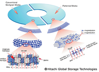
Present Recording media
Modern computer hard-disk media have a continuous thin film of a Co-based alloy coating on their surfaces, comprising many abutting crystals, or ‘grains’. Typical grain diameters for current media are less than 10nm. A few hundred grains form a small area that is magnetised either parallel, or anti-parallel to the read/write head, during the data recording process. These form magnetic regions (named ‘bits’), each of which is used to encode a single binary unit of information, corresponding to a 0 or 1.
Limitations
Increasing magnetic data storage density is the main goal for the hard-disk drive industry. To increase the storage density, the grain size needs to be reduced. But controlling grain size and position can be difficult and imposes limits on the achievable storage density. Additionally, one large grain can spontaneously re-magnetise a smaller adjacent grain, leading to data loss. This effect can propagate through a recording medium over time, as more grains become magnetised in the ‘wrong’ direction, causing further data loss.
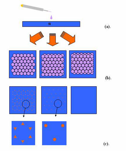
Figure 1(a), (b) and (c) shows the process used for manufacturing patterned storage media. (a) and (b) show the coating processes for different numbers of nano-spheres, while (c) shows the resultant patterned media. Further details are included in the main text.
Patterned Media
An alternative approach, called patterned media, is to have non-magnetic areas surrounding islands of magnetic material, which can be magnetised in the same manner as the grains described above. The location and size of the islands can be more easily controlled and this can potentially allow more data to be stored in a smaller area, without the data loss described above. The islands have to be just the right size, however. Too large and the packing density is reduced; too small and they will spontaneously re-magnetise in a different direction, due to their thermal energy.
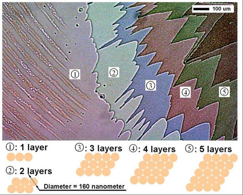
Figure 2 shows a sample after it has been coated in nano-spheres (not visible at this magnification). The different colours denote the number of nano-sphere layers. Only one or two layer is required for the process described in the text.
Pattern Media Production
How do we make the magnetic islands on a recording medium like a hard disk drive? There are several approaches, one of which involves placing regularly sized spheres onto a flat surface, as shown in figure 1(a) and (b), and then coating a magnetic material onto the gaps between the spheres, via a complex process called nano-sphere lithography. This forms the magnetic islands that can store data, see figure 1(c). Figure 2 shows an image of a sample coated in one or more layers of nano-spheres. Controlling the size, distribution, and shape of the magnetic islands is challenging and forms part of our ongoing research in this area.