Transmission Electron Microscopy
The Nanocentre currently houses two TEM instruments. A modified JEOL 2200 FS TEM/STEM for aberration corrected measurements with environmental capabilities, and a JEOL 2010 for more routine analysis. Details of both instruments are provide below.
In addition a new state-of-the-art environmental aberration corrected STEM microscope is due to be installed in 2022, which will be equipped with a post column EELS spectrometer and large solid angle EDX detection system.
In-situ Aberration Corrected Environmental TEM/STEM Microscope
This is a 200kV Field Emission Transmission and Scanning Transmission Electron Microscope (TEM/STEM) with Cs Aberration Correctors for both TEM and STEM with 1 Å resolution, achieving single atom imaging sensitivity.
This instrument is based on a JEOL 2200 FS TEM/STEM system with third order spherical aberration correctors for both TEM and STEM modes has been in-house modified with an open cell environmental chamber for dynamic in-situ experiments under operational conditions of controlled temperature (room temperature to 1100 C) in a gas environment (O2, N2 and H2) with pressure up to 10 Pa.
The instrument is equipped with:
- Thermo scientific 100mm2 silicon drift EDX detector
- In column Omega type Electron Energy filter
- A High Angle Annular Dark Field (HAADF) STEM detector
- A Bright Field (BF) STEM detector
- In situ MEMS heating/biasing holders single and double tilt (DENS solution)
- In situ heating liquid cell holder single tilt (Protochips)
- In situ furnace heating single tilt holders (Gatan)
- High dynamic range CCD ultrascan camera
- Fast frame acquisition Orius camera for dynamic TEM
- Turbo molecular pump vacuum system
- Wide gap HRP objective lens pole piece
- Remote operation
Please contact the Advance Electron Microscopy Director (Prof. Vlado Lazarov) and the Research Officer (Dr. Leonardo Lari) for further details about access.
Example Applications:
Catalyst Nanoparticles
![]()
The Environmental STEM allows the study of oxidation and reduction cycles relevant to the regeneration of nanoparticle catalysts that can be deactivated due to sintering or poisoning. In these images nickel nanoparticles were studied via in situ high angle annular dark field imaging in the presence of oxygen and hydrogen atmospheres. Chem. Mater. 2018, 30, 197-203
Nanostructures and interfaces
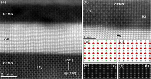
Aberration-corrected atomic resolution Z-contrast scanning transmission electron microscopy of device structures reveals that annealing at 350 °C and 500 °C creates partial B2/L21 and fully L21 ordering of electrodes, respectively. Interface structural studies show that the Ag/Co2FexMn1−xSi interface is more ordered compared to the Co2FexMn1−xSi/Ag interface. This study suggests that by improving the atomic ordering and strain at the interfaces, further enhancement of the magnetoresistance of CFMS-based current-perpendicular-to-plane spin valves is possible. J. Phys. D: Appl. Phys. 2014, 47, 322003.
Biominerals
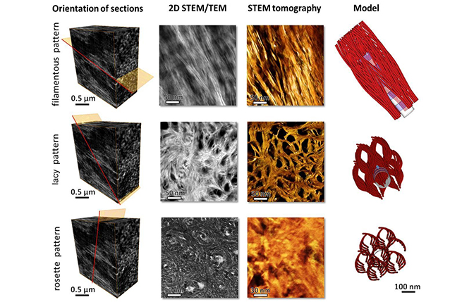
A proposed model of crystal organization in bone was compared with 2D projections obtained from TEM and STEM (second column of panels) and the tomogram reconstructed from the STEM tilt series (amber-colored, third column of panels). Science 2018, 360, eaao2189.
JEOL 2010 TEM
The JEOL 2010 is a conventional transmission electron microscope (TEM) with a lanthanum hexaboride (LaB 6 ) thermionic electron source, ultra-high resolution pole-piece (UHR) and Gatan 794 MultiScan close-coupled device (CCD) digital camera.
The 2010 is used for basic TEM imaging, which includes bright-field imaging (BF), dark-field imaging (DF), high-resolution (HREM) imaging and electron diffraction. There is no STEM. Further, a silicon-drifted lithium (Si(Li)) energy dispersive X-ray detector allows point analysis of the chemical composition of near-nanometre sized samples.
The 2010 is equipped with:
- Gatan MultiScan 794 CCD camera - 1024 × 1024 pixels
- UHR pole-piece with low spherical (Cs = 0.5 mm) and chromatic (Cc=1.0 mm) aberrations. The point resolution is 0.19 nm.
- Single tilt (±25 o ) and double tilt (±25 o ) specimen holders
- Thermo-Scientific Si(Li) EDS detector and Noran System Seven analysis system
This instrument is suitable for simple metrology, diffraction patterns and basic chemical analysis by EDX.
Please contact the Director (Dr Steve Tear) or the Experimental Officer (Dr Jonathan Barnard) for further details about access. You can also email nanocentre-access@york.ac.uk.
Example Applications
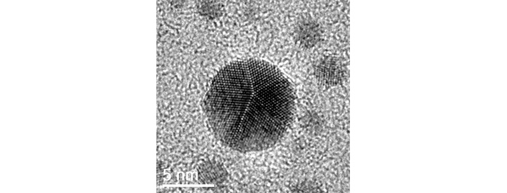
This is a gold nano-particle sitting on a thin amorphous carbon film. The atomic spacing are clearly resolved, showing the icosahedral (5-fold) arrangement of crystalline grains within.
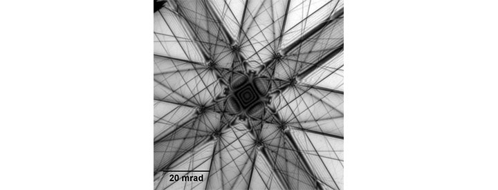
This is a large angle convergent beam electron diffraction pattern (LACBED) which shows how the transparency of a single crystal of silicon changes depending on the beam orientation. Dark lines correspond to electrons meeting the Bragg diffraction condition, which scatter strongly out of the beam. Dark interference fringes near the centre reflect the 4-fold symmetry of the arrangement of silicon atoms as the electrons pass through. The fringes and dark lines testify to the wave-nature of electrons passing through the crystal.
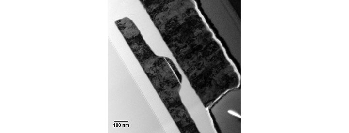
A bright-field image of a single junction device which was found, cut out, and thinned using the Nova 200 FIBSEM. Together, the FEI Nova FIBSEM and the JEOL 2010 TEM allow us to do site-specific TEM imaging of larger devices and materials.