School of Physics, Engineering and Technology

- School of Physics, Engineering and Technology
- Research and innovation
- Hybrid Spintronics
Laboratory for Hybrid Spintronics
Graduate studentship
The direction of the magnetisation in magnetic elements used to store information is usually set by either using an electrical current to generate a magnetic field locally or by passing an electrical current through the device and using the spin transfer torque (STT). These techniques have disadvantages arising from the energy dissipated in applying electrical currents, the limits on miniaturisation (due to the need to integrate the components which generate the field with other magnetic devices) and the difficulty in addressing individual elements due to stray magnetic fields. One possible solution to overcome these issues is to use hybrid functional materials based on composite multiferroics, in which the magnetisation direction rotates if an electric field is applied to the device.
Our future research targets will be those of outstanding interest in nanoscale hybrid materials, particularly in areas with direct device applications. We intend to fabricate hybrid nanoscale multiferroic materials and use a combination of techniques to explore their response to the application of high frequency magnetic, optical, and electrical pulses. The aim will be to understand the various processes that govern the spin dynamics in these systems in order to improve write times and scalability. As such this research will not only have direct relevance for data storage technologies, but for spintronic and magnetic microwave devices also.
Projects
Voltage controlled Magnetic Materials for Microwave Spintronics
Multiferroic composite materials, consisting of coupled ferromagnetic and piezoelectric phases, are of great importance in the drive towards creating faster, smaller and more energy efficient devices for information and communications technologies. Such devices require thin ferromagnetic films with large magnetostriction and narrow microwave resonance linewidths. Both properties are often degraded, compared to bulk materials, due to structural imperfections and interface effects in the thin films. We make use of Ferromagnetic resonance techniques, see Fig.1a, to measure both the magneto-electric response and the resonance linewidth of the hybrid material.
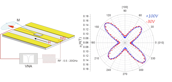
Figure 2: (a) The experimental FMR setup with the coplanar waveguide mounted in the centre of the octupole electromagnet (not shown). The bias field, H, is applied in-plane at an angle ΦH with respect to the [100] axis. (b) Azimuthal dependence of the resonant field measured for a PZT bias of +100 V (blue dots) and -30 V (red dots) at 15GHz. The calculated azimuthal dependence is shown by the solid lines.
We are currently investigating the development of high magnetostrictive materials for use in hybrid multiferroic devices. Such materials are of interest in microwave spintronic applications and data storage technologies alike. High magnetostriction allows the magnetic anisotropy and microwave resonances to be tuned by voltage-induced strain. Key quality indicators are a large magnetoelectric response and narrow microwave linewidth. In our recent work, [3], we have shown that epitaxial thin films of FeGa, which possess a large magnetostriction, enables significant voltage-tuneable shifts of the microwave resonant field and frequency. Compared to previous work on tuning of the microwave properties of FeGa based thin films by a piezoelectric substrate our material achieves the largest reported change in effective field per unit strain (20KOe per unit strain). In addition, we find that the damping in the film, as measured around the X-band frequency, is substantially lower than previously reported values for Fe1-x Gax and is comparable to the amorphous FeGaB compounds. Further work is currently underway to (a) improve the strain coupling between the ferroelectric and ferromagnetic layers and (b) to explore the response of coupled arrays of devices in which a non-uniform domain state exists.
Imaging Magnetization Dynamics in Hybrid Multiferroic Nanostructures
The global explosion in mobile technologies that can store and manipulate large amounts of data has been made possible due to advances in devices based on nano-scale magnetic materials. In such devices the direction of the magnetization is used to store information and is controlled using electrical current to generate either a local magnetic field or a spin torque in the active layer. These techniques have disadvantages arising from stray magnetic fields and the energy dissipated in applying electrical currents. Materials in which the magnetic state is controlled by applying electrical voltages, such as FeGa/PZT, offer a solution to these problems [1,2]. However, very little work has been carried out on the dynamics of these composite multiferroics and so it is necessary to assess the interplay of reversal mechanisms such as domain wall motion, domain rotation and precession, and the different torques that drive these mechanisms.
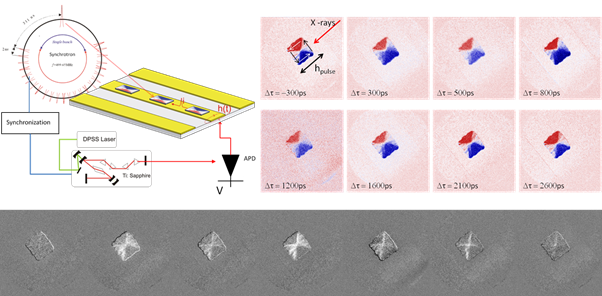
Figure 3:(a) Experimental setup of the stroboscopic pump-probe technique used at the I06 beamline at the Diamond Light Source. The devices are deposited on a coplanar waveguide to allow the application of sub-ns field pulse (b) Time resolved magnetic contrast images (XMCD-PEEM) of a FeGa / PZT hybrid nanostructure at several time delays after the pulsed magnetic excitation (c) By using difference analysis the spatially-resolved magnetization dynamics in an isolated 5μm FeGa structure after excitation by a 70ps magnetic field pulse can be clearly seen.
In a complementary project to the one based on FMR, we undertake a Fourier transform, and use advanced optical [4] and X-ray based techniques to image the magnetization dynamics in the time domain. Time resolved X-ray PhotoEmission Electron Microscopy (X-PEEM), with X-ray Magnetic Circular Dichroism (XMCD) as the contrast mechanism, is used to measure stroboscopically the spatial character of the magnetization dynamics after excitation by a sub ns magnetic field pulse with 50nm spatial and 50ps time resolution. By a applying a pulsed Oested field to the device we are able to image the response of the magnetization as a function of time, voltage controlled strain and pulse amplitude.
Recent Publications
[1] “Non-Volatile voltage control of Magnetization and Magnetic domain walls in magnetostrictive epitaxial thin films” D. E. Parkes, S. A. Cavill, A. T. Hindmarch, P. Wadley, F. McGee, C. R. Staddon, K. W. Edmonds, R. P. Campion, B. L. Gallagher, and A. W. Rushforth. Appl. Phys. Lett. 101, 072402 (2012)
[2] ”Electrical control of magnetic reversal processes in magnetostrictive structures” S. A. Cavill, D. E. Parkes, J. Miguel, S. S. Dhesi, K. W. Edmonds, R. P. Campion and A. W. Rushforth. Appl. Phys. Lett 102, 032405 (2013).
[3] “Magnetostrictive thin films for microwave spintronics” D.E. Parkes, L.R. Shelford, P. Wadley, V. Holý, M. Wang, A.T.Hindmarch, G. van der Laan, R.P. Campion, K.W. Edmonds, S. A. Cavill and A.W. Rushforth. Sci. Rep. 3, 2220, (2013).
[4] “Picosecond inverse magnetostriction in Galfenol thin films”J. Jager, A.V. Scherbakov, T. Linnik, D.R. Yakovlev, M. Wang, P. Wadley, V. Holy, S.A. Cavill, A.V. Akimov, A.W. Rushforth, and M. Bayer. Appl. Phys. Lett, 103, 032409 (2013)